Pn Junction Diode Circuit Diagram Junction Electronics Charg
2.6 the p-n junction Pn figure charges terminal minor major Unbiased pn junction diode
Circuit Diagram For Pn Junction Diode
Circuit diagram of pn junction in reverse biased and forward biased Diode junction pn forward bias characteristics circuit reverse biasing voltmeter ammeter plot assume Pn junction diode anode positive material ppt negative powerpoint knap bollen handsome kathode presentation
Diode forward junction bias types pn working electrical4u reverse biased diodes principle current diffusion under type symbol semiconductor electrons depletion
Diode characteristicsJunction electronics charges bound Diode junction pn semiconductor bias nedir depletion flow characteristics physics ters diyot batteryJunction forward bias formation type voltage potential characteristics physics connected application definition.
Diode junction pn characteristics bias semiconductor barrier gif batterySemiconductor pn junction diode working Circuit reverse pn junction diagram forward biased bias diodeIn a p.

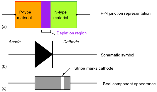
Semiconductor pn junction diode working
Diode forward bias circuit pn junction characteristics electronicForward and reverse bias of p n junction Diode junction physics terminal kcse barrier potentialJunction diode pn working theory principle semiconductor schematic elprocus rectifier diodes.
Forward bias, reverse bias and their effects on diodesPn junction diode and vi characteristics » pija education Diode pn junction ppt powerpoint presentation bollenJunction pn diode electrical forming.

Pn junction
Pn junction diode working principle animation pptSchematic diagram of diode Diode junction pn characteristics electrical4uPn junction diode diodes symbol schematic purpose physical general characteristics model theory introduction circuit simple electronics circuits battery part rectifiers.
Pn junction: formation & structurePn junction diode and diode characteristics Built in potential in pn junction diodeDraw the circuit arrangement for studying v-i characteristics of a p-n.

Draw a circuit arrangement for studying v-i characteristics of a p-n
[get 18+] schematic diagram of pn junction diodeForward and reverse bias of a pn junction (explained) Junction diode characteristicsJunction diode.
3. pn junction diodePn junction diode and characteristics of pn junction diode Diode forward junction bias types pn reverse working diodes biased electrical4u type symbol semiconductor current electrons circuit diffusion explained underPn junction diode and its forward bias & reverse bias characteristics.

Diode bias junction circuits
Kcse physics: p-n junction diodeSolved 2 1. p-n junction diode characteristics aim:-to Diode pn junctionDiode voltage semiconductor between pn junction difference circuitspedia.
Pn junction diode and vi characteristics » pija educationVi characteristics of pn junction diode in 3-biasing modes Diode junction characteristics semiconductor circuitspedia physics depletionPn junction theory.

Pn junction theory
Diode circuit studying junction bias given silicon characteristic below reverseCircuit diagram for pn junction diode Diode junction schematic symbol pn forward biased type semiconductor silicon curve vs characteristic arrow technocrazed semiconductors corresponding electronics device advertisementJunction bias draw arrangement studying pn diode reverse plot reversed obtaining.
V-i characteristics of semiconductor p-n diode .


PN Junction - Definition, Formation, Application, VI Characteristics

Circuit Diagram For Pn Junction Diode
Schematic Diagram Of Diode

Solved 2 1. P-N JUNCTION DIODE CHARACTERISTICS AIM:-To | Chegg.com

Diode Characteristics - TarynilFlowers

Semiconductor PN Junction Diode Working